
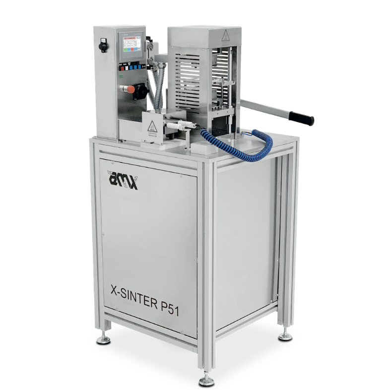
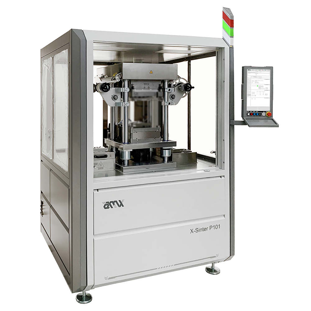
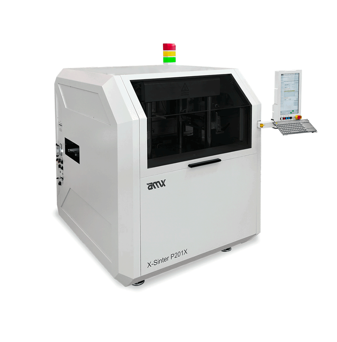
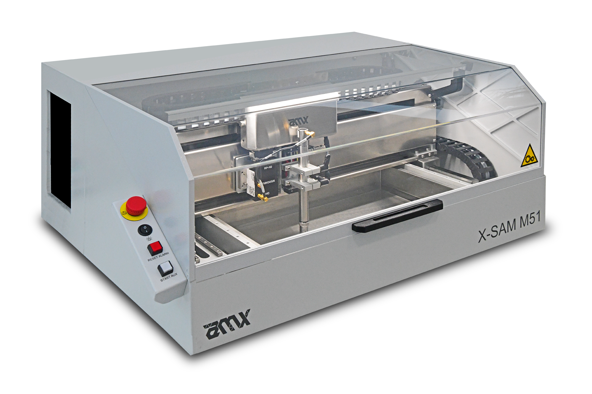
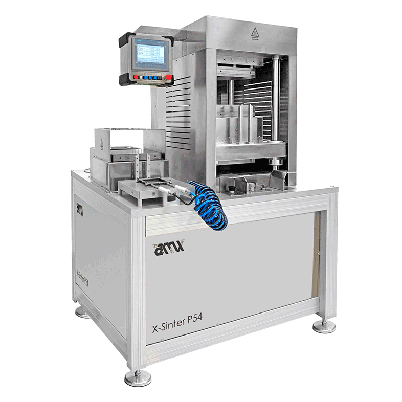

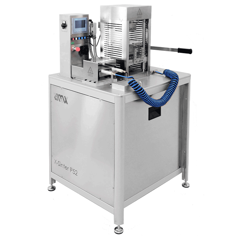







Wafer Lamination products
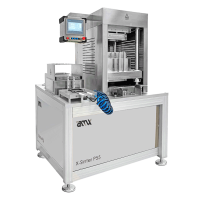
Wafer/Panel process
Wafer-Level Sintering: Wafer bonding, Wafer Lamination, Die on Wafer (D2W) and IC on Wafer for Heterogeneous Integration.
As the semiconductor industry hits the physical limits of traditional transistor scaling, Advanced Packaging and Heterogeneous Integration (HI) have become the primary drivers for performance gains.

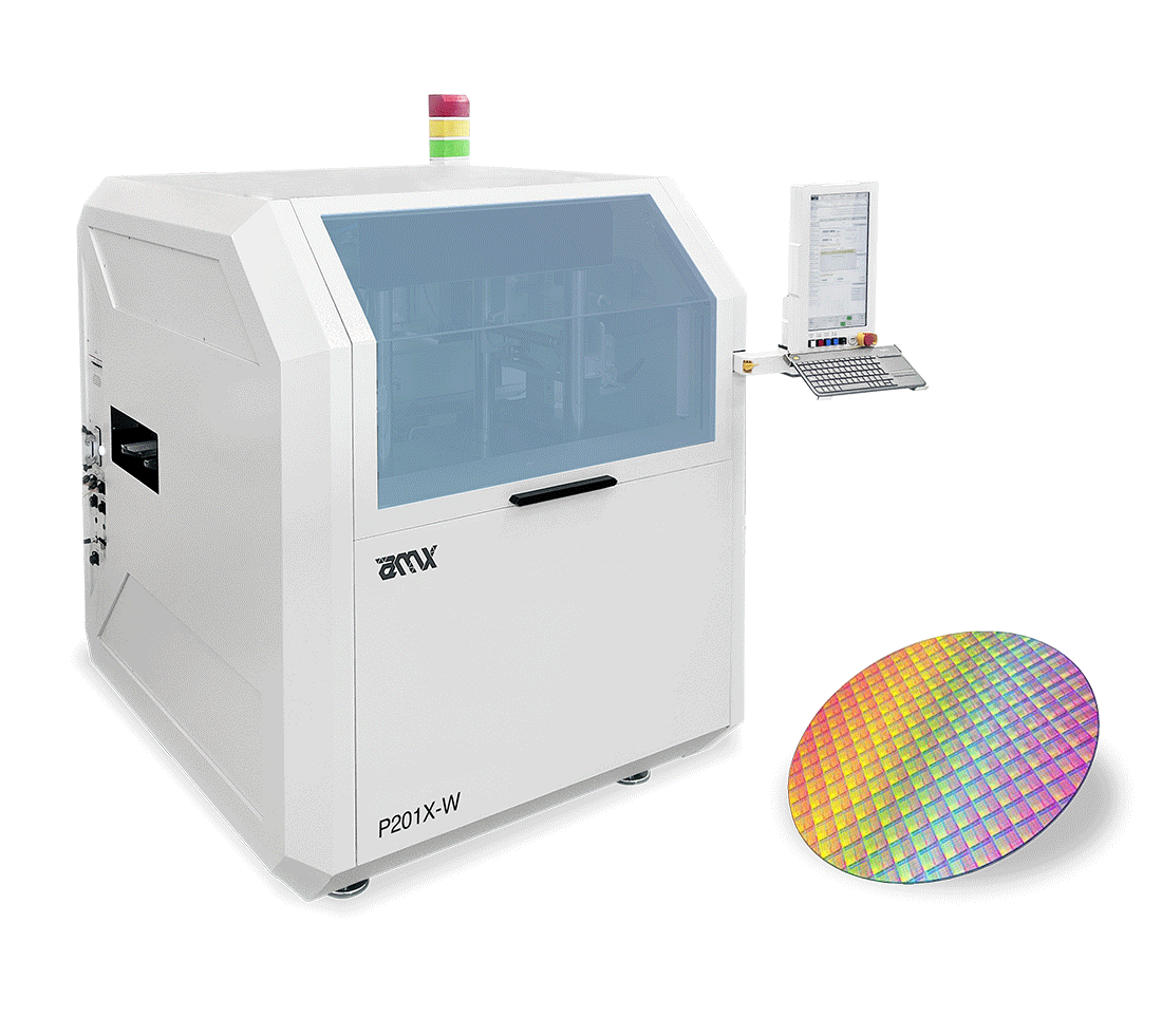
The AMX P201X-W and P201X-LP series provide a high-precision platform for Die-to-Wafer (D2W) and Wafer-to-Wafer (W2W) bonding, essential for next-generation System-on-Chip (SoC) and System-in-Package (SiP) manufacturing.
The equipment is available in several versions in order to be suitable both for back-end and for front-end cleanroom environments up to ISO3.
Supported Processes
- Wafer to Wafer / Panel (W2W)
- SiC and wafer lamination (TIM or PEP) and Cu foil on SiC Wafer
- Die to Wafer / Panel (D2W)
- IC to Wafer / Panel (D2W)
- Hybrid bonding
- Wafer Lamination
- Wafer to Wafer Bonding
Technical Advantages & High-Yield Features
Optimized Throughput and Cycle Time
Designed for high-volume mass production, the system is available in two versions: carrier or carrier-less handling concept. Utilizing integrated load ports for FOUP/FUOP to FOUP transitions, a robotic end-effector performs direct wafer picking, notch alignment, and data collection.
Precision Thermal Management
The P201X-W series offers the best thermal tool uniformity, critical for managing the different coefficients of thermal expansion in complex 3D stacks. Controlled preheating and cooling cycles minimize thermal stress, preventing micro-damage during the bonding of sensitive components.
Oxidation-Free Processing (N2 and/or Forming Gas with certified sensors)
To support high-density interconnects and Hybrid Bonding (copper-to-copper diffusion, copper pressure sintering or any exposed copper components or wafer copper layers), the system operates within a full inert atmosphere cabinet. By maintaining Nitrogen (N2) levels with oxygen concentrations below 100 ppm, the system prevents copper oxidation from room temperature, to process, to cooling at room temperature again. Utilizing Forming Gas can also reduce any eventual oxidation presence.
Patented Micropunch Technology
AMX exclusive Micropunch System allows for selective and differentiated pressure on individual components. This technology can accommodate variations in component thickness (e.g., SiC, IGBT, and NTC sensors) and different target pressure within the same cycle, ensuring perfect force distribution across the wafer / panel, even in case of non-planar surfaces.
Adaptive Tooling with Planetary Load Cells
The lower tool features an embedded patented planetary load cell system providing automated compensation for substrate or wafer tilting up to ±0.300 mm. This "adaptive tool" provides radiant force feedback (kN) and guarantees a Total Thickness Variation (TTV) of less than ±0.010 mm, effectively eliminating defects like voids, delamination, and die cracks.
Front-End Cleanroom Compatibility
The AMX units feature integrated roof-top HEPA (or ULPA) filtration and a sealed cabinet to maintain strict cleanliness standards. This prevents particle contamination, which is the leading cause of defective interconnects in micron-pitch packaging.
Smart Factory Integration & Compliance
- Inert Atmosphere Load Port: Direct FUOP to FUOP handling with integrated RFID for automated data collection.
- SEMI 300: Fully compatible with smart factory / Fabs wafer automation and SECS/GEM single-protocol communication for factory-level control and traceability.
- Global Certifications: All systems are CE and UL Marked, ensuring compliance with international safety and quality standards for global deployment.
Supported Advanced Packaging Applications
-
 Thermo-Compression Bonding (TCB) for IC-on-Silicon Wafers.
 -
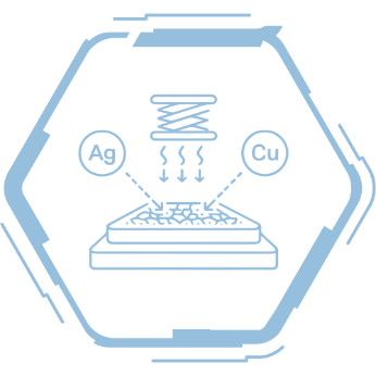 Embedded Die and Double-Side Cooling (DSC) modules.
 -
 Silicon Carbide (SiC) and Gallium Nitride (GaN) power electronic packaging.
 -
 Chiplet-based integration for AI data centers and automotive communication.
Advanced Applications & Technology Focus
While the X-Wafer P200 W offers maximum inline flexibility, its core strength lies in solving the most critical challenges of high-density semiconductor packaging. It bridges the gap between classic sintering and high-end frontend/mid-end bonding requirements.
Engineered for W2W & D2W Sinter-Bonding
The system is optimized for cutting-edge Wafer-to-Wafer (W2W) integration as well as high-precision Die-to-Wafer (D2W) bonding. Whether you are processing homogeneous or heterogeneous semiconductor materials, the X-Wafer P200 W ensures a reliable, high-yield thermocompression sinter-bond.
The Micro-Punch Advantage for Wafer Processing
Traditional rigid flat presses often fail during large-area wafer bonding due to wafer warpage or TTV (Total Thickness Variation), leading to voids or destructive micro-cracks.
Our patented Micro-Punch system utilizes a matrix of individual punches to apply independent, perfectly uniform pressure across the entire wafer surface.
It dynamically adapts to thickness variances, securing a 100% void-free bond layer without putting mechanical stress on fragile SiC or GaN structures.
Key Integration Capabilities
- Material Compatibility: Fully capable of handling both Advanced Silver (Ag) and Oxygen-controlled Copper (Cu) sintering processes.
- Cleanroom & Fab-Ready: Available with standard Loadport (SMIF/FOUP) configurations and automated AGV handling interfaces.
- Advanced Data Logging: Deep integration into factory MES systems, recording precise pressure, temperature, and time profiles for every single bonding sequence to guarantee automotive-grade traceability.
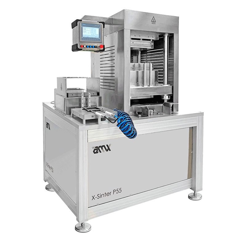
Our patented technology
Discover AMX Automatrix Micro-Punch System
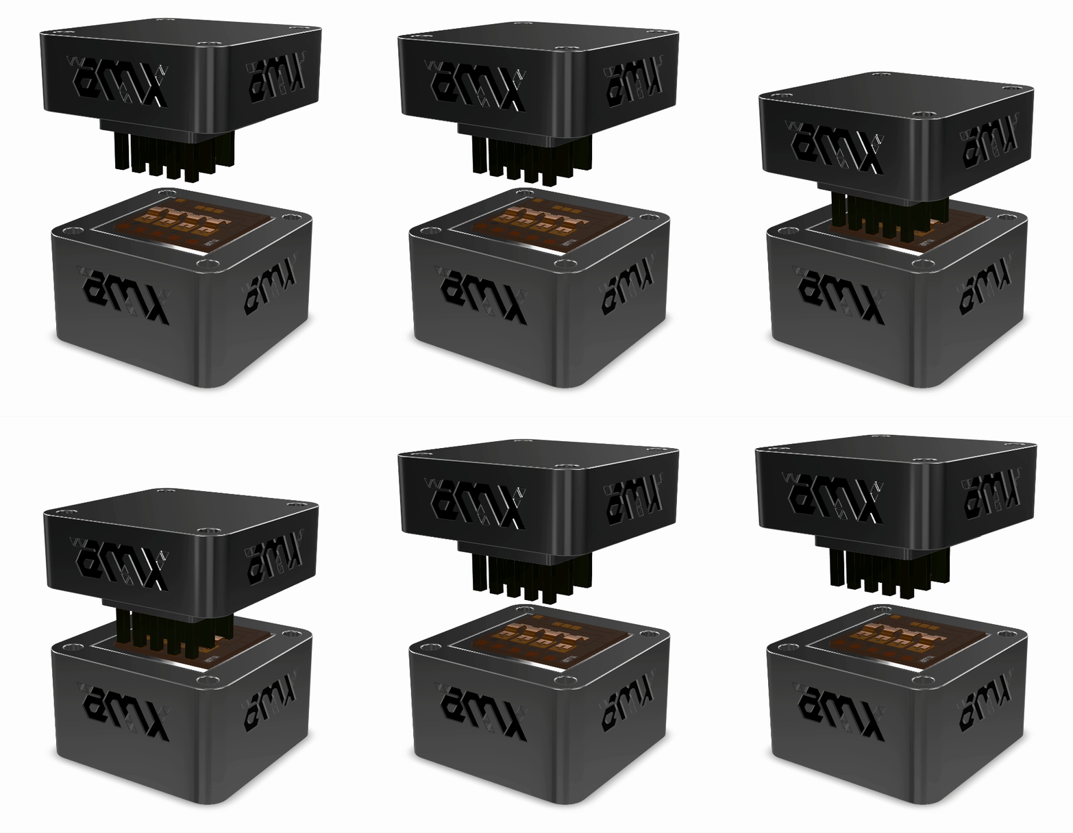
AMX Automatrix worldwide patented a unique sintering tool for its sintering press, the ‘Micro-Punch’ able to press individually and with a dedicated pressure every single component on the substrate.
Discover more