


Technologies for Next-Generation Power Devices
The increasing demand for components characterized by high power density and the shift towards Wide Bandgap (WBG) semiconductors, such as the next generation of IGBT (Si), Silicon Carbide (SiC) and Gallium Nitride (GaN), requires the use of robust and reliable interconnection technologies. This necessity extends across critical industrial sectors beyond automotive, including railway traction systems (public transport), aerospace and defense, energy transfer systems GRID (UPS, Solar, Wind), and high-frequency communication infrastructures such as 5G and high-performance computing (HPC).
Datacenters and AI applications are also moving in this direction, driven by the persistent technical requirement to increase power density (W/m3) and maximize system efficiency. To ensure the performance and reliability demanded by these harsh environments, pressure sintering has emerged as the industry's preferred die attach solution
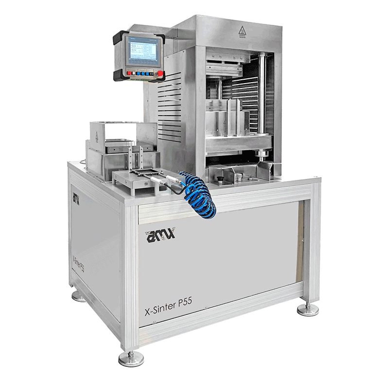
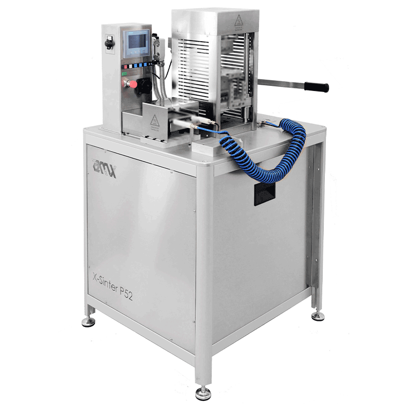
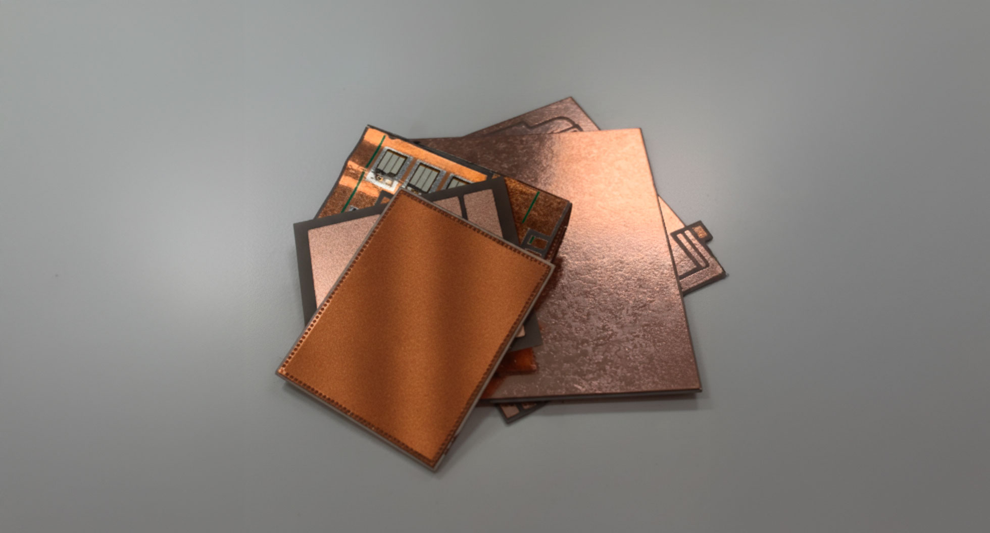
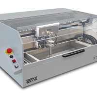
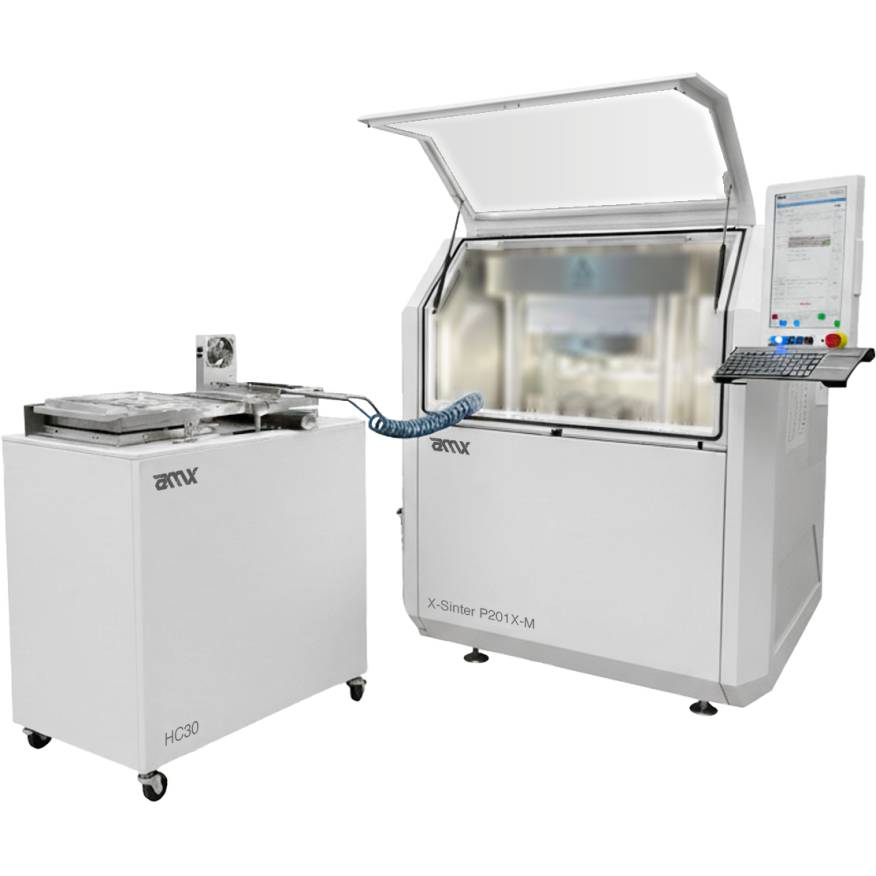
Pressure sintering (PS) is a heat treatment process applying simultaneous heat and external uniaxial pressure (typically ranging from 5 MPa to 40 MPa) to metallic particle pastes (Silver/Copper). This technique is essential for achieving reliable die attach solutions capable of continuous operation at junction temperatures exceeding 200°C. The application of pressure drives densification, critically reducing residual porosity, often below 10%. This results in a superior bulk metallic microstructure guaranteeing exceptional thermal conductivity (e.g., sintered Ag ∼300 W/(m⋅K)) and low electrical resistivity (∼2 μΩ⋅cm).
Datacenters and AI applications are also moving in this direction, driven by the persistent technical requirement to increase power density (W/m3) and maximize system efficiency. To ensure the performance and reliability demanded by these harsh environments, pressure sintering has emerged as the industry's preferred die attach solution
Pressure sintering (PS) is a heat treatment process applying simultaneous heat and external uniaxial pressure (typically ranging from 5 MPa to 40 MPa) to metallic particle pastes (Silver/Copper). This technique is essential for achieving reliable die attach solutions capable of continuous operation at junction temperatures exceeding 200°C. The application of pressure drives densification, critically reducing residual porosity, often below 10%. This results in a superior bulk metallic microstructure guaranteeing exceptional thermal conductivity (e.g., sintered Ag ∼300 W/(m⋅K)) and low electrical resistivity (∼2 μΩ⋅cm).
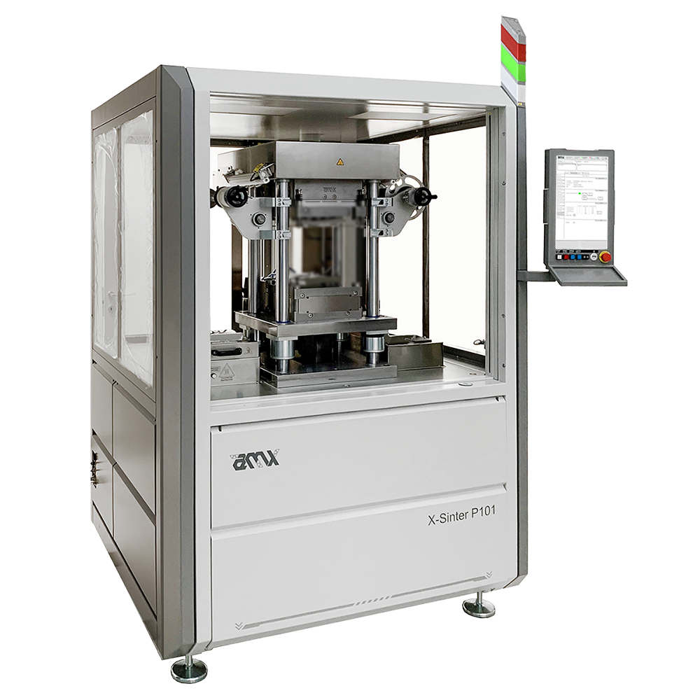
Die sintering on ceramic substrates
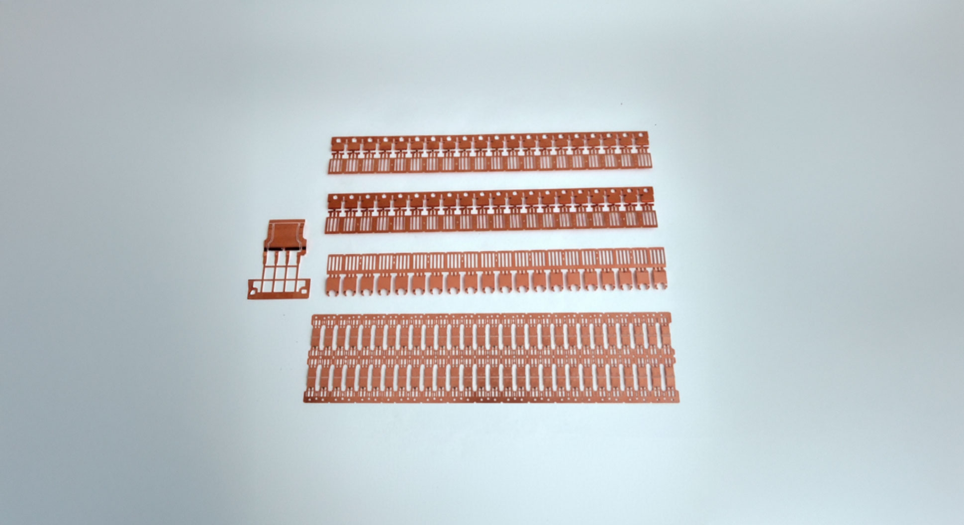
Core application involving the bonding of SiC/IGBT/MOSFET dies to substrates (DBC or AMB). It supports the simultaneous sintering of diverse components (e.g., NTC thermistors, IGBR resistors, clips, spacers, and pillars) within a single production cycle.

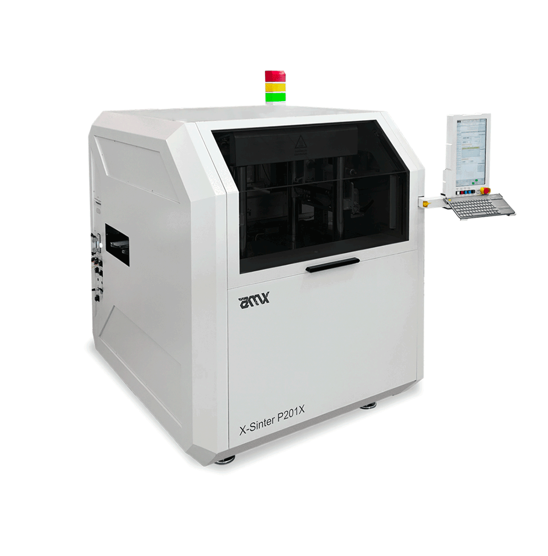
Clip sintering on die top side and ceramic substrate
Clip sintering, Cu foil and other component on top of die top side.
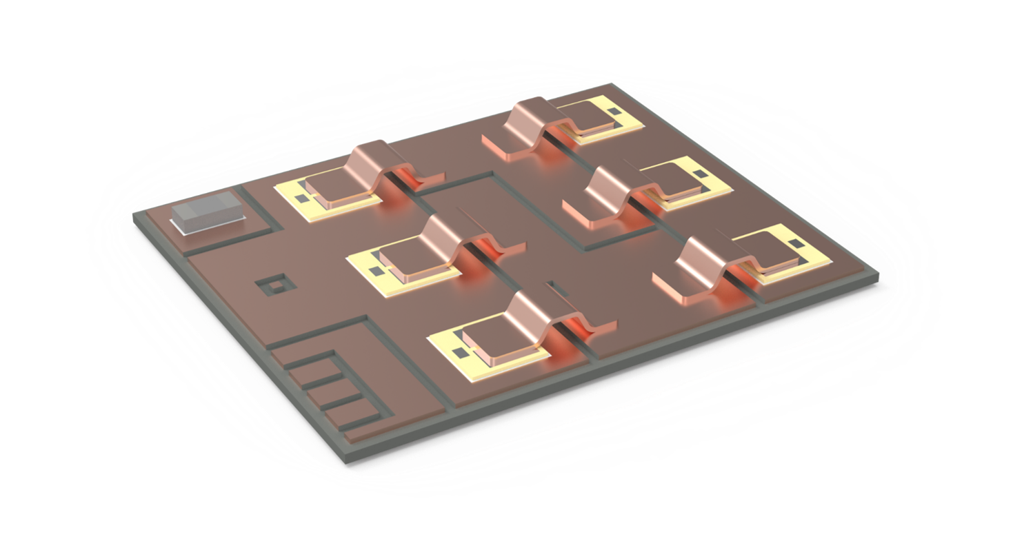
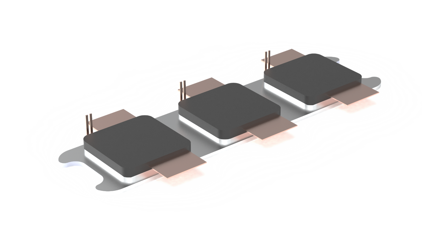
Double Side Cooled (DSC) Packages
Forming complex multi-layered 3D structures where the entire package, including the dies, sensors, frames, and the second DBC on top, is sintered to optimize bi-directional heat dissipation.

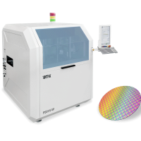
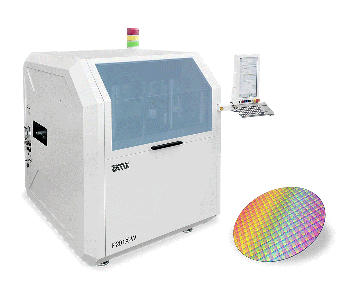
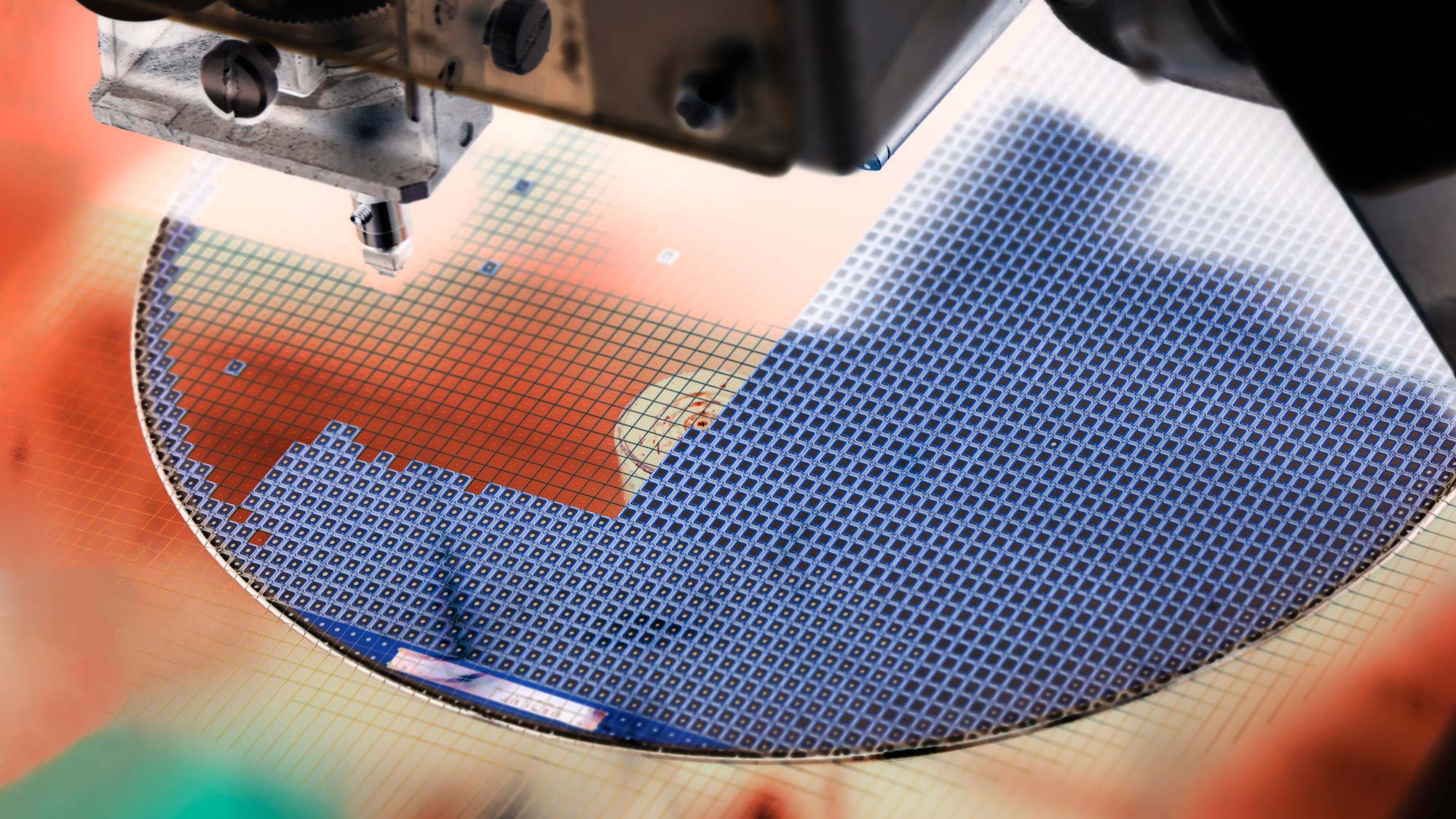
Wafer Level Applications
Used in front-end, mid-end, and back-end processes, enabling high-performance and significantly improving time to market.