


Boundaries are being pushed in all engineering sectors, but few more so than with regards to power electronics.
For every problem solved in the power semiconductor industry, it seems that at least one other is introduced. Where performance is concerned,the goals are typically to increase power density and to operate at higher switching frequencies. These goals have been met by moving from silicon (Si) to wide bandgap materials, and silicon carbide (SiC) has become extremely popular.
To date, only relatively simple structures such as diodes and mosfets have been fabricated in SiC and are commercially available. These tend to be in standard packaging and that is what limits their operating temperature range. However, many applications are calling for more advanced
structures and/or the ability to cope with higher temperatures.
In theory, any semiconductor device structure that can be fabricated in Si can, with suitably adjusted manufacturing processes, be made in SiC and a far higher (5x to 10x) power density should be achievable.
Tests are necessary to confi rm that theory can be put into practice. The University of Warwick, for example, has a dedicated Power Electronics Applications and Technology in Energy Research (PEATER) group for
research into SiC power electronics and the development of fabrication processes for bipolar SiC power semiconductor devices. Expertise covers fundamental materials research, device simulation and optimisation,
fabrication, characterisation, packaging and reliability testing.
It is worth noting that thermal cycling is an important factor. For example, AEC-Q100, the qualifi cation test for packaged integrated circuits for automotive applications, details four ambient operating temperature ranges. The widest range is -40oC to 150oC. But SiC-based devices will, subject to packaging, be able to operate at far higher temperatures. It is not hard to imagine a SiC die at the heart of an automotive component in a vehicle working in a cold environment cycling from sub-zero temperatures to more than 300oC several times a day.
As part of its work with the EPSRC (Engineering and Physical Sciences Research Council) Centre for Power Electronics, the university has already produced SiC insulated-gate bipolar transistors (IGBTs) with breakdown voltages of 10kV, noting that silicon IGBTs are typically rated up to about 5kV. In addition, full gate control has demonstrated the viability of the technology for applications including high voltage DC transmission.
Testing and characterisation are performed using a SemiProbe PS4L probe system and other equipment in the university’s dedicated wide bandgap semiconductor characterisation facility. Thanks to a degree of automation, the tests are highly repeatable and are producing a wealth of data. This means that for any given manufacturing process and desired device performance goals it is possible to determine the yield from a SiC wafer.
Make the connection
To benefi t from a SiC semiconductor die’s ability to operate at a high temperature – noting that SiC power semiconductors can operate with junction temperatures in excess of
500oC – it is best to attach it to a substrate, such as copper, which will provide good heat dissipation. However, solder cannot be used because it has a melting point lower than the kind of temperatures the
SiC die might reach. For example, the popular lead-free SAC alloy melts at about 230oC. Also, at only a
few tens of Watts per meter-Kelvin (W/(m.K)), solder is not that good a thermal conductor.
An alternative to soldering is sintering, a manufacturing process that is a combination of heat and pressure. Silver is currently the most popular sintering material. Its melting point is about 960oC and the thermal conductivity of a sinter paste is very good (between 130 and 250W/(m.K)).
The sintering process is as follows. A sinter paste comprising monometallic particles, of less than 1μm in size, and a resin are printed (in a similar way to solder paste) onto a substrate in patterns corresponding to the shapes and locations of the SiC dies. The substrate is heated to evaporate the resin and the dies are placed.
Pressure, which can be up to a few tens of MPa, is applied as a downwards force. It serves two purposes. First, a lower temperature can be used to bond the materials, yet the bonds achieved will
be able to operate at a higher temperature in the fi eld.
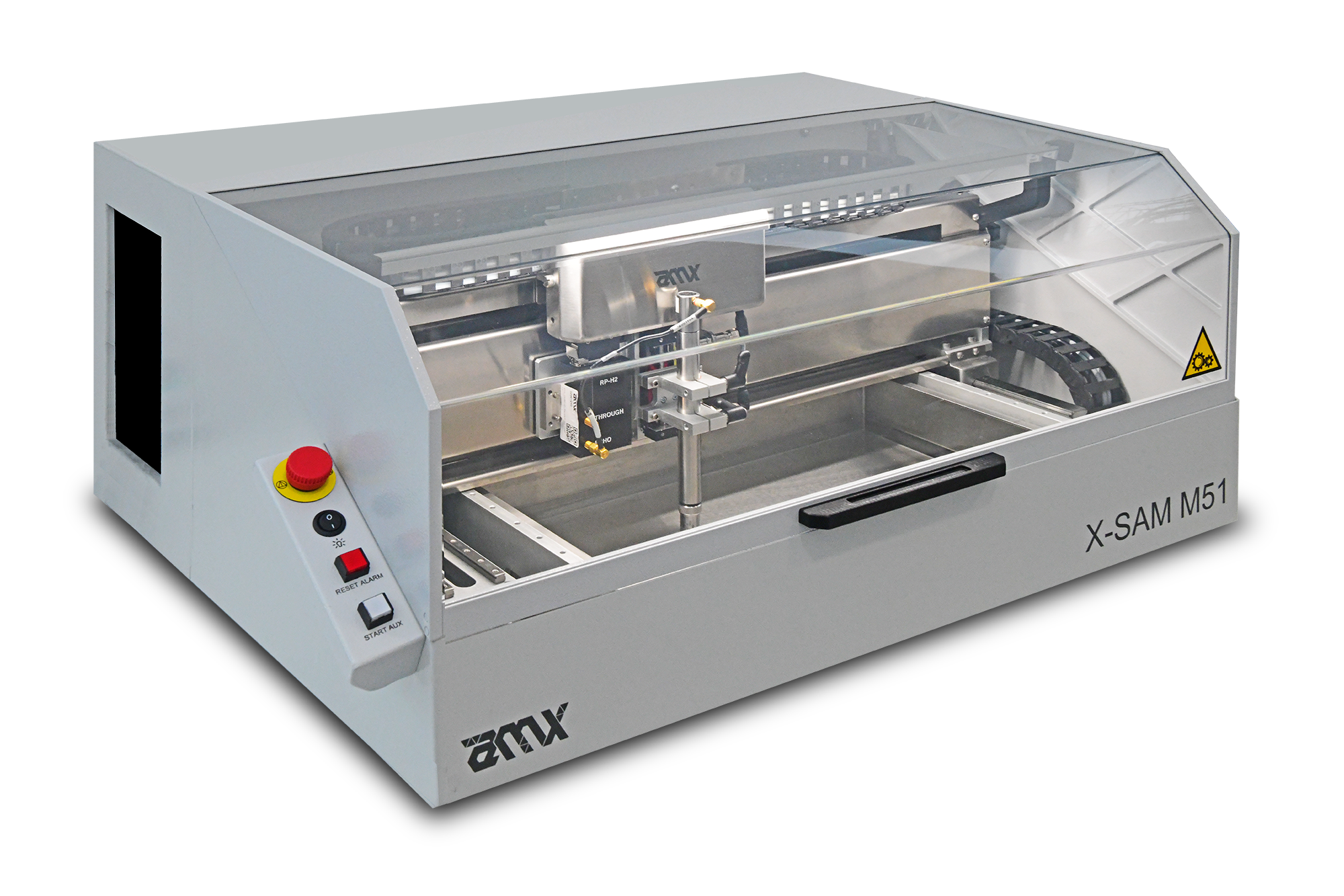
Second, it reduces the risk of voids, which can lead to delaminating and cracking over time. Note: checking for the presence of voids requires the use of a scanning acoustic microscope as x-ray equipment does not work; the power required to penetrate the metallic substrate is so high it makes the die virtually invisible.
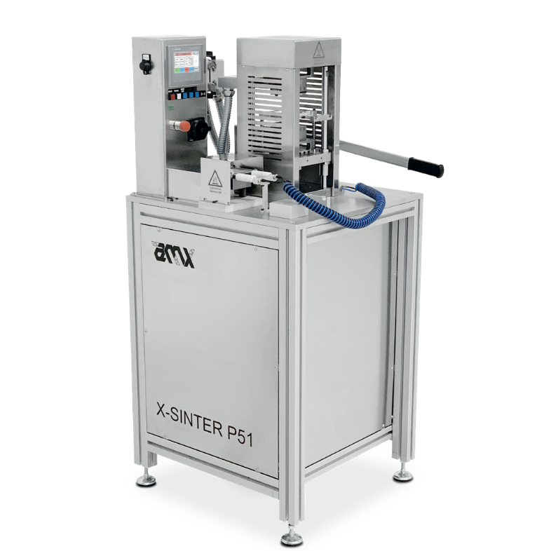
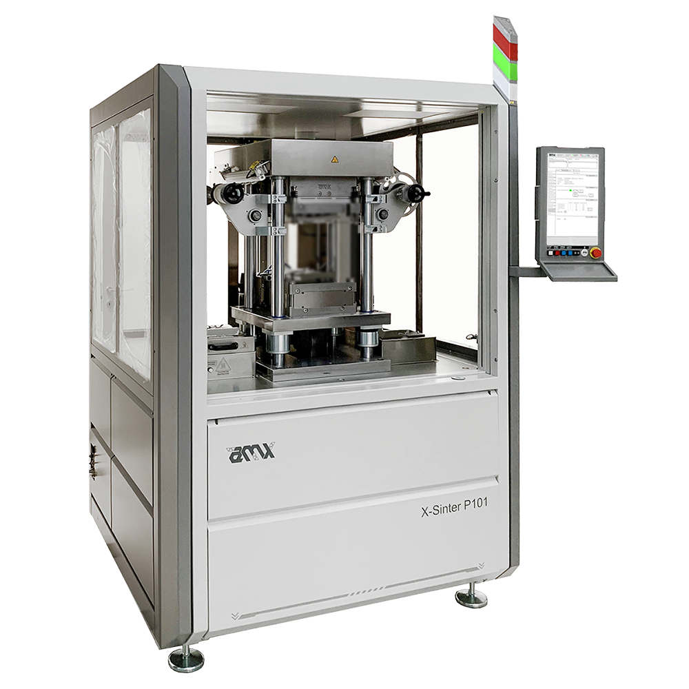
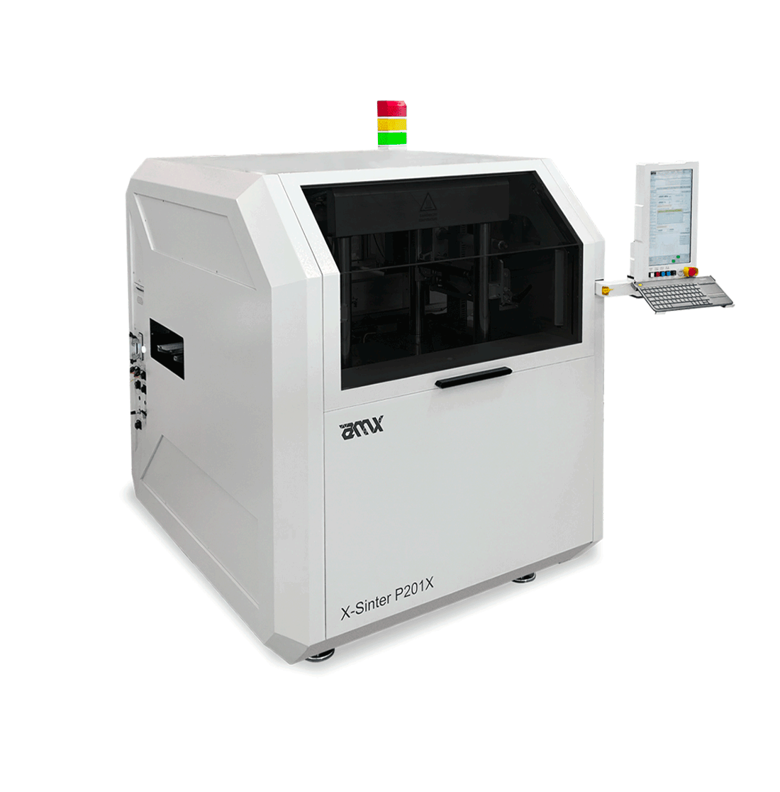
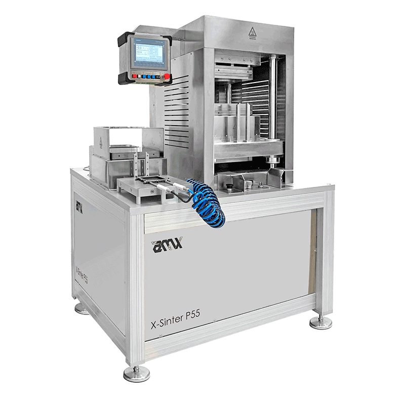
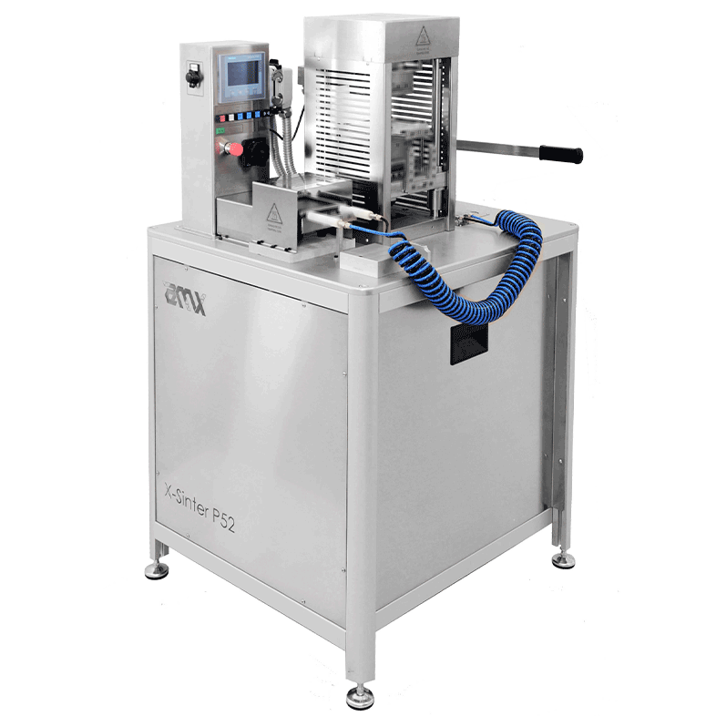
Sintering for die attach is a relatively new technology. For example, the North East’s Driving the Electric Revolution Industrialisation Centre (DER-IC) – funded by UK Research and Innovation and set up in 2020 – has just taken delivery of an AMX P100 sinter press. It employs a Micro-Punch system that allows equal force to be applied to multiple dies of varying thickness. Compared to using a single (fl at) punch, this mitigates against the risk of voids forming beneath thinner dies.
DER-IC will provide open access facilities and aims to bring together the UK’s technology and manufacturing expertise in electrifi cation research and development. It is believed DER-IC is the fi rst facility in the UK to take delivery of a sinter press as advanced as the AMX P100.
Supply chain
In many cases, those developing next generation SiC-based power devices are in unknown territory. They have volume (space) and ideal performance characteristics in mind, but can such a device be made?
Few organisations will want to invest in cap-ex equipment, which is why the services off ered by the North East’s DER-IC have such an important role to play. The Compound Semiconductor Applications Catapult,
a DER-IC for the Southwest and Wales, off ers services too. Its Power Electronics Laboratory is heralded as one of the country’s most advanced and comprehensive modelling, characterisation, integration and
validation facilities for power electronics innovation. It also provides advanced packaging capabilities for power electronics.
Distributors are doing their part too. For instance, Inseto has a Process Development Laboratory at its headquarters in Andover. In 2021, the company invested in a Kulicke & Soffa Asterion wedge bonder to join
its materials test and plasma cleaning equipment. A major OEM of power ICs is, at the time of writing, using the facility. Also, several companies have been using the facility recently to develop battery cell wirebonding processes. These companies range from existing battery pack manufacturers exploring new processes to start-ups doing prototype runs. In all cases they have access to equipment they cannot yet aff ord to invest in. That, plus access to expertise.
Empowered
In summary, the production of next generation power semiconductor devices requires new types of equipment and processes. But that is to be expected considering the use of materials such as SiC. What is interesting is the amazing level of collaboration between industry and academia, and roles being played by OEMs and distributors to de-risk programmes. Engineers have access to expertise that is confi rming if custom (and potentially high volume) power devices can be fabricated. And if so, how.
Autors: Matt Brown and Andy Longford
Read the article: click here.
You can download the full magazine here (subject to account access)