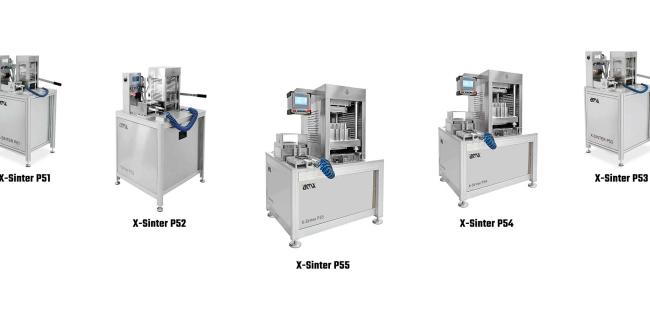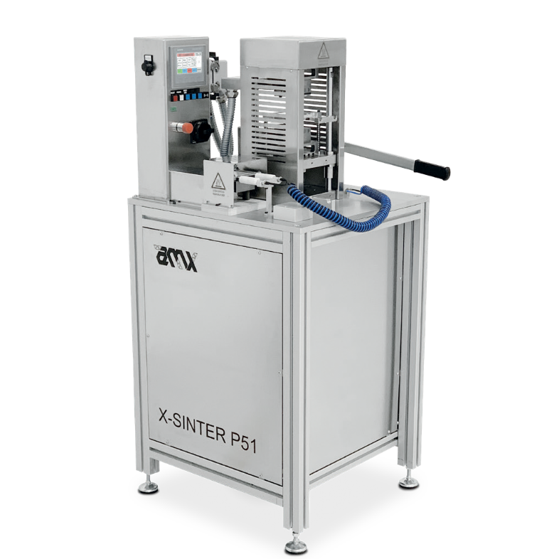
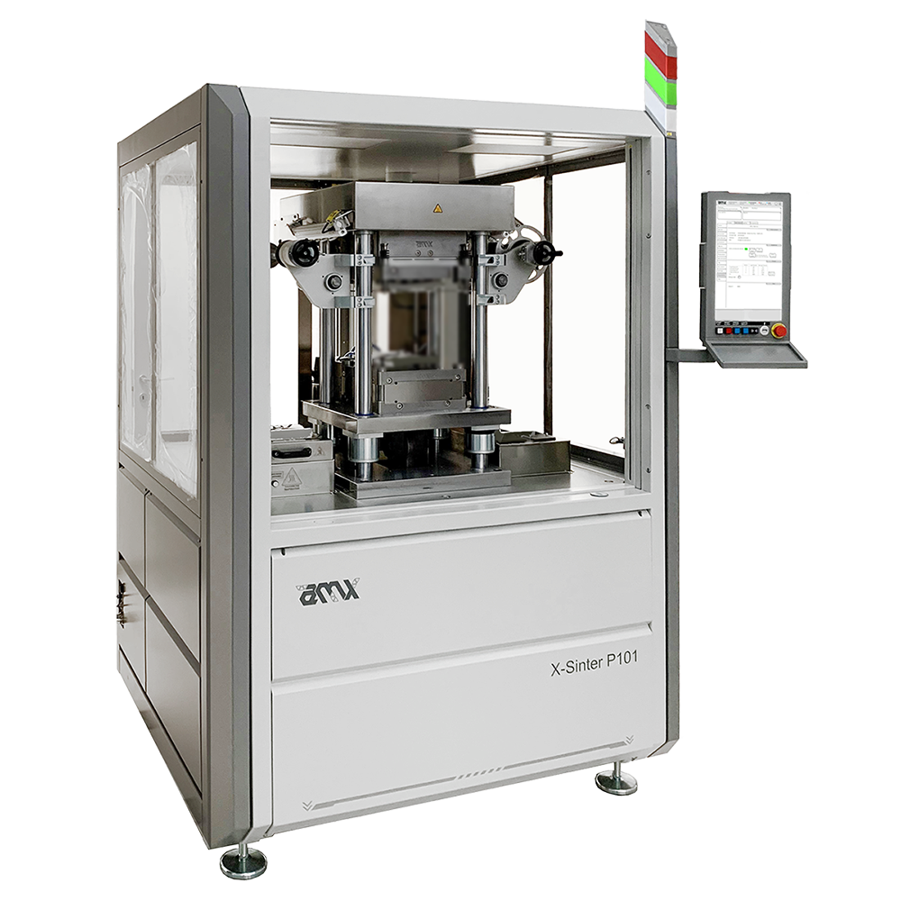
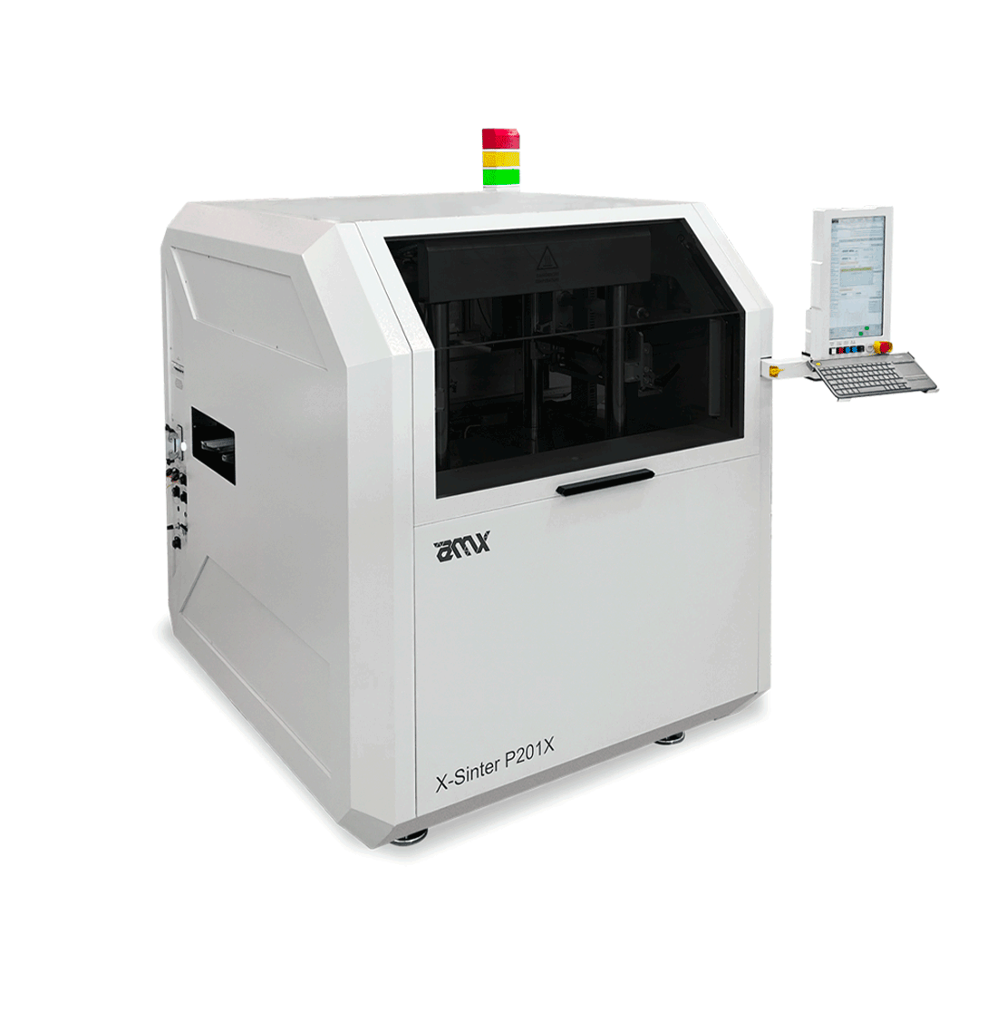
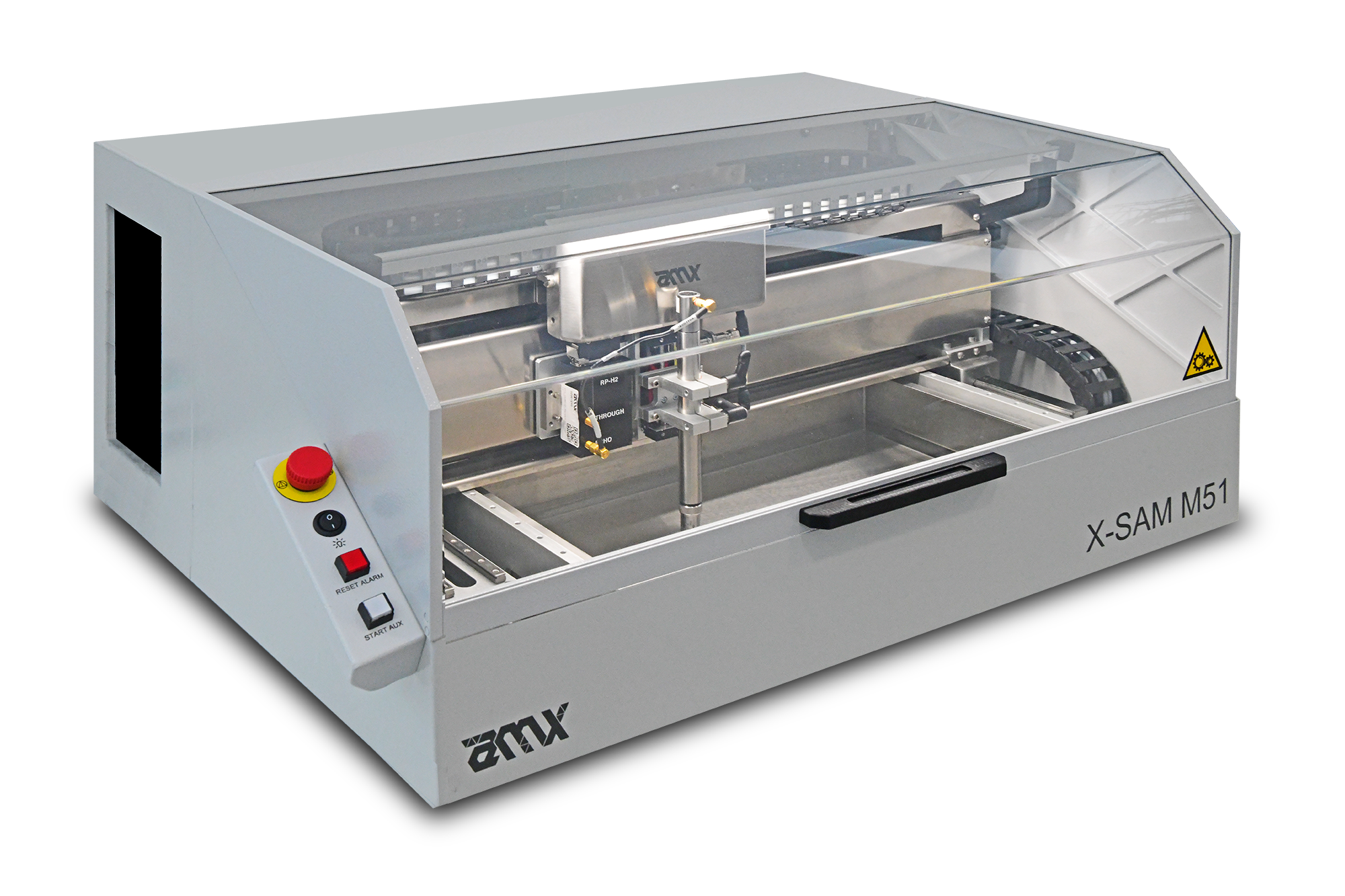
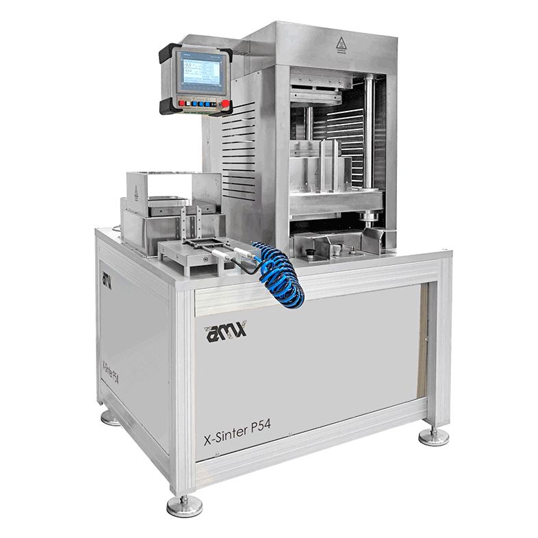

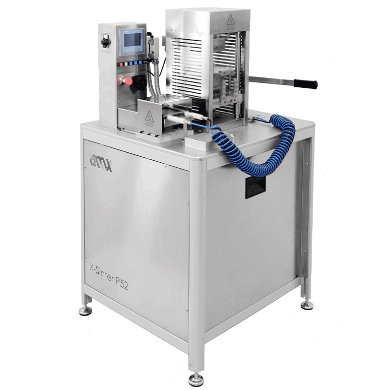


AMX Automatrix at IEEE IEMT 2026: scalable pressure-assisted sintering, bonding, and lamination for 300 mm wafers and next-generation power packages.
Note on Publication and Acknowledgments
An earlier version of this work was presented as an Invited Technical Talk at the 41st IEEE International Electronics Manufacturing Technology (IEMT) Conference 2026 (IEEE IEMT 2026), held in Putrajaya, Malaysia.
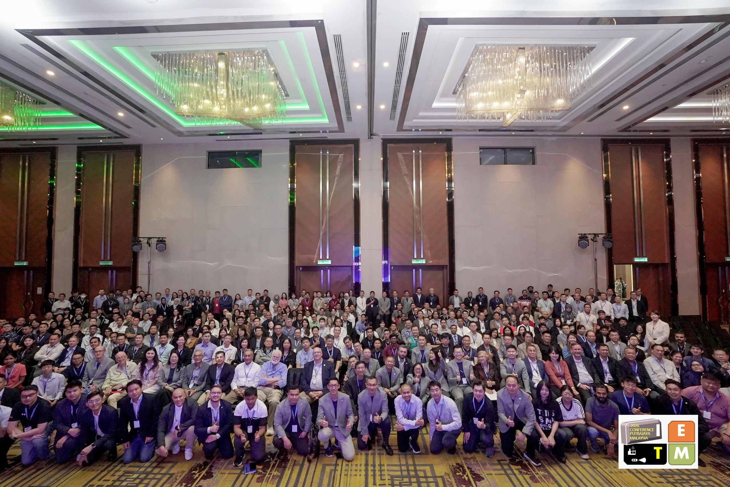
We would like to express our sincere gratitude to the Malaysian technical and academic community, as well as to the local organizers and industry experts, for their continuous contributions to advanced semiconductor packaging. Special thanks are extended to the IEEE Malaysia Section and the IEEE CPMT (Components, Packaging, and Manufacturing Technology) Malaysia Chapter for fostering an exceptional collaborative ecosystem during our stay and technical sessions in Malaysia.
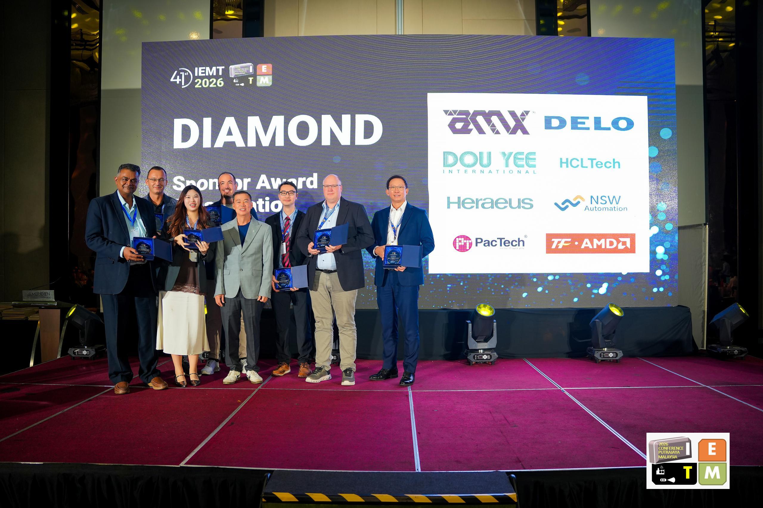
This expanded paper details the technological evolution of AMX Automatrix's pressure-assisted bonding and wafer-processing platforms. It outlines the transition from laboratory-scale R&D towards full-scale semiconductor mass manufacturing, highlighting advanced packaging techniques, carrier-less FOUP handling, cleanroom environment control, and dynamic thermomechanical tooling architectures.
Abstract
The physical and economic cost limitations of traditional package scaling are pivoting the semiconductor industry toward advanced packaging and heterogeneous integration.
Hybrid Bonding and Electrical Resistance
Hybrid bonding improves electrical performance by replacing traditional solder-based micro-bumps with direct copper-to-copper interconnects. This approach achieves a 90% reduction in electrical resistance compared to soldered solutions. The reduction is primarily driven by smaller, shorter connections that allow for a 16x increase in interconnect density, enabling superior energy efficiency and lower latency for high-performance applications such as AI data centers. Direct copper-to-copper interconnects, as well as Ag pressure-assisted sintering, also eliminate solder-related defects.
A Scalable Pressure-Assisted Bonding Ecosystem
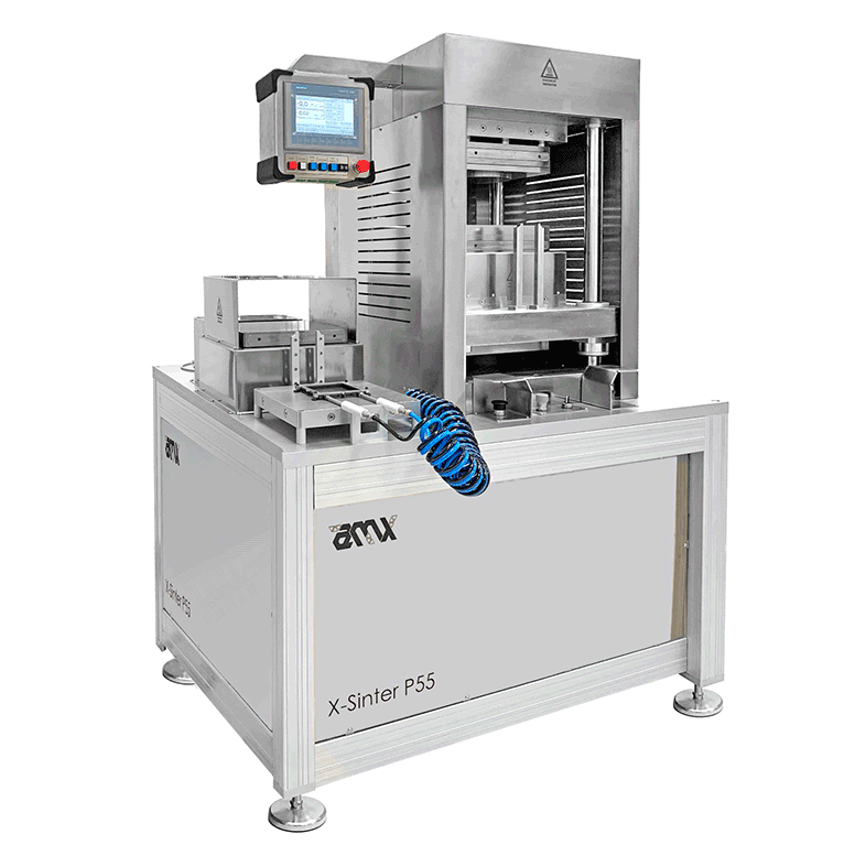
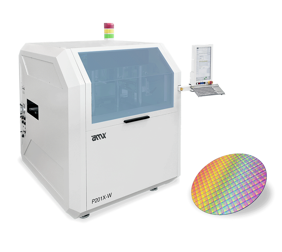
This paper details the implementation of AMX Automatrix's scalable pressure-assisted bonding ecosystem, spanning from manual R&D platforms (P55) to versatile prototyping systems (P201XM), up to fully automated high-volume production lines (P201X-W). Designed for high-precision Die-to-Wafer (D2W), Wafer-to-Wafer (W2W), and substrate-level joining across back-end, middle-end/post-fab, and advanced assembly environments, these platforms support wafers up to 300 mm (12-inch) and panels up to 300x300 mm.
Proprietary Mold Technology and the Patented Micropunch System
A central innovation lies in the tool's proprietary mold technology, now scaled to support 12-inch (300 mm) wafers and 300x300 mm panels. At the core of this evolution is the patented Micropunch system, which establishes a new benchmark for thermomechanical performance. This technology enables the simultaneous application of selective, differentiated pressure across discrete components, allowing heterogeneous components to be integrated while ensuring optimal bonding profiles regardless of:
- Pressure variance: precise management of disparate target pressures within a single cycle.
- Form factor versatility: seamless handling of ultra-miniature components alongside large-scale IC packages.
- Coplanarity challenges: compensation for height deviations across the assembly.
Adaptive Lower Tooling Architecture
Furthermore, the patented adaptive lower tooling architecture is engineered to accommodate substrate tolerances. It ensures absolute pressure uniformity and optimized thermal transfer across the sintering interface, reaching a TTV (Total Thickness Variation) of less than ±0.010 mm and compensating for substrate/wafer tilting up to ±0.250 mm. By maintaining uniform force distribution and achieving a tilting accuracy of less than 0.005 mm, the system prevents die cracking and ensures robust interconnects for complex packages, such as embedded dies and Double-Side Cooling (DSC) modules.
Elevate Your Packaging Yield and Thermal Reliability
Whether you are scaling SiC power module production or building advanced AI chiplet architectures, our engineering team is ready to support your process requirements.
The full version of the paper and the related presentation are available on request: get in touch with us to receive them.